


-- FUJIFILM Corporation today announced the successful completion of a new building for development and evaluation at the Shizuoka Factory of FUJIFILM Electronic Materials Co., Ltd. (FFEM), the core company that leads Fujifilm’s semiconductor materials business, with operations commencing in November.This investment strengthens the company’s capabilities for performance and quality evaluation of development products, accelerating the development of new materials for advanced and next-generation semiconductors and ensuring a stable supply of high-quality products. Fujifilm will further accelerate the growth of its semiconductor materials business to meet the rapidly increasing demand for semiconductors supporting advanced information society, such as those for AI data centers.
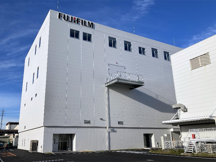
Exterior Photo of New Building
In recent years, the semiconductor market has grown rapidly due to the spread of AI, 5G, and IoT, with particularly strong demand for advanced semiconductors such as those used in AI applications. Fujifilm’s semiconductor materials business has expanded its sales by approximately 1.7 times from FY2021 to FY2024, becoming one of the core businesses driving the growth of the Fujifilm Group. To support this growth, Fujifilm has invested over 100 billion yen in facilities from FY2021 to FY2024, and plans to invest an additional 100 billion yen or more from FY2025 to FY2026.
The new building at the Shizuoka Factory is equipped with state-of-the-art evaluation equipment in a high-cleanliness cleanroom, enhancing quality evaluation functions for development and production. AI image recognition technology has been introduced to inspect fine particles contained in semiconductor materials, improving analysis accuracy and establishing an advanced quality control system utilizing AI. Furthermore, a department promoting digital transformation (DX) has been established in the new building to support the expansion of digital technologies such as AI in manufacturing processes, thereby improving product quality and ensuring stable supply.
As part of business continuity planning (BCP), the building adopts an RC column-head seismic isolation structure and locates the cleanroom 12 meters above ground to prepare for potential flooding.
The Shizuoka Factory collaborates with global R&D and production bases to support customers’ cutting-edge process technology development, not only for the Japanese market but worldwide.
With the launch of the new building, Fujifilm will accelerate the development of advanced resists for EUV (Extreme Ultraviolet)*1, ArF*2, NIL*3, PFAS-free*4 materials, and the world-leading WAVE CONTROL MOSAIC™*5, contributing to the advancement of next-generation semiconductors.
Previous investments have also strengthened the development and mass production systems for core materials such as polyimides*6 for next-generation semiconductor packaging. Fujifilm will continue to expand production capacity and develop technologies to meet diverse customer needs, including increasing demand for AI semiconductors.
Through this investment in the new building at the Shizuoka Factory, Fujifilm will further strengthen its development and production systems for semiconductor materials, leading the growth of the advanced and next-generation semiconductor market, which is expected to double by 2030, and accelerating the expansion of its semiconductor materials business and overall group growth.
Fujifilm is a global supplier of photoresists*7, photolithography-related materials*8, CMP slurries*9, post-CMP cleaners*10, thin-film chemicals*11, polyimides, high-purity process chemicals*12, and other process materials for semiconductor manufacturing from front-end to back-end processes. Fujifilm is also expanding globally with products such as WAVE CONTROL MOSAIC™, which includes color filter materials for image sensors.
Fujifilm will continue to contribute to the development of the semiconductor industry by providing one-stop solutions to solve customers' issues through its broad product lineup that covers almost all areas of the semiconductor manufacturing process, from cutting-edge to legacy nodes, as well as by leveraging its global stable supply system with manufacturing bases in major countries in Japan, the United States, Europe and Asia and its advanced research and development capabilities.
- *1 Advanced lithography technology using extreme ultraviolet (EUV) light, necessary for generations with features finer than 10 nanometers.
- *2 An exposure method using ArF (argon fluoride) excimer laser light (wavelength 193nm), which is currently the most widely used advanced lithography technology.
- *3 Nanoimprint lithography. A technology in which a mask (mold) with circuit patterns is pressed onto the resist applied to a semiconductor wafer, like a stamp, to transfer and form the circuit patterns.
- *4 PFAS refers to a collective term for perfluoroalkyl compounds, polyfluoroalkyl compounds, and their salts, as defined in the OECD's 2021 report “Reconciling Terminology of the Universe of Per- and Polyfluoroalkyl Substances: Recommendations and Practical Guidance.” Accordingly, the claim ‘PFAS-Free’ denotes the absence of substances falling within this defined group.
- *5 General term referring to a group of functional materials for controlling electromagnetic light waves in a broad range of wavelengths, including photosensitive color materials for manufacturing color filters for image sensors such as CMOS sensors, used in digital cameras and smartphones. WAVE CONTROL MOSAIC is a registered trademark or trademark of FUJIFILM Corporation.
- *6 A material with strong heat resistance and insulation properties, used for forming semiconductorsprotective films and rewiring layer.
- *7 Material used to coat wafer substrate when circuit patterns are drawn in the process of semiconductor manufacturing.
- *8 Development solutions, cleaners and other materials used in the photolithography process of semiconductor manufacturing.
- *9 A proprietary formulation containing an abrasive that uniformly planarizes semiconductor surface, which contains a mixture of wires and insulation films of varying hardness.
- *10 Cleaners used after polishing with CMP slurry to remove particles, minute metal fragments and organic residues while protecting the metal surface.
- *11 Materials for forming low-dielectric insulation films.
- *12 High-purity chemicals used in the cleaning and drying processes. The chemicals are employed to remove contaminants during the cleaning and drying stages of semiconductor manufacturing, as well as to eliminate metals and oils during the etching process.
New Building Overview

Media Contact
FUJIFILM Holdings Corporation
Corporate Communications Division, Public Relations Group
Tel: +81-3-6271-2000
Release ID: 89176946

 Google
 RSS
RSS